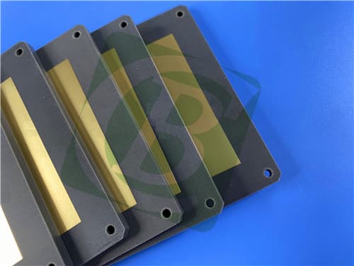
F4BTMS255 2-Layer 1.6mm PCB – 60mil Ceramic-Filled PTFE with Immersion Gold for Aerospace & RF1. Introduction to F4BTMS255 2-Layer 1.6mm PCB The F4BTMS series represents an upgraded version of the F4BTM series, achieving significant technological breakthroughs in material formulation and manufacturing processes. Enriched with substantial ceramic content and reinforced with ultra-thin, ultra-fine glass fiber cloth, this material demonstrates substantial performance improvements and offers a broader range of dielectric constants. As a high-reliability material suitable for aerospace applications, it can effectively replace similar imported products. By incorporating minimal ultra-thin glass fiber cloth and large amounts of uniformly distributed special nano-ceramics mixed with polytetrafluoroethylene resin, the material minimizes the negative effects of glass fiber on electromagnetic wave propagation. This innovative composition reduces dielectric loss, enhances dimensional stability, decreases X/Y/Z anisotropy, expands usable frequency range, improves electrical strength, and enhances thermal conductivity. Additionally, the material exhibits excellent low thermal expansion coefficient and stable dielectric temperature characteristics. The F4BTMS series features RTF low roughness copper foil as standard, which reduces conductor loss while maintaining excellent peel strength, and is compatible with both copper and aluminum bases. 2. Key Features (F4BTMS255) Dielectric constant (Dk) of 2.55 ±0.04 at 10GHz 3. Benefits Minimal electromagnetic wave propagation interference
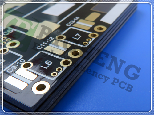
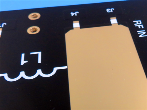
4. PCB Construction Details
5. PCB Stackup (2-Layer Rigid Structure) Copper_layer_1 - 35 μm 6. PCB Statistics: Components: 28 7. Typical Applications Aerospace equipment and space cabin systems 8. Quality Assurance Artwork Format: Gerber RS-274-X |
Get a Quick Quote
Fill in the form below and our engineers will reply within 24 hours with technical specifications and pricing for F4BTMS255 2-Layer 1.6mm PCB – 60mil Ceramic-Filled PTFE with Immersion Gold for Aerospace & RF.